
Most CPU-sockets interfaces are based on the pin grid array (PGA) architecture, in which short, stiff pins on the underside of the processor package mate with holes in the socket. To minimize the risk of bent pins, zero insertion force (ZIF) sockets allow the processor to be inserted without any resistance, then grip the pins firmly to ensure a reliable contact after a lever is flipped.
As of 2007, several current and upcoming socket designs use land grid array (LGA) technology instead. In this design, it is the socket which contains pins. The pins contact pads or lands on the bottom of the processor package.
In the late 1990s, many x86 processors fit into slots, rather than sockets. CPU slots are single-edged connectors similar to expansion slots, into which a PCB holding a processor is inserted. Slotted CPU packages offered two advantages: L2 cache memory could be upgraded by installing an additional chip onto the processor PCB, and processor insertion and removal was often easier. However, slotted packages require longer traces between the CPU and chipset, and therefore became unsuitable as clock speeds passed 500 MHz. Slots were abandoned with the introduction of AMD's Socket A and Intel's Socket 370.
Socket 563 is a microPGA CPU socket used exclusively for low-power (16 W and 25 W TDP) Athlon XP-M processors (Models 8 & 10).
This socket can usually be found on laptops and requires a low-power mobile part in a special 563-pin µPGA package which is different from the Socket A (453 pin) package used for other Athlon processors.
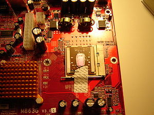
There exists desktop computer motherboards equipped with socket 563. PCChips is known to have marketed such a board, the M863G Ver3 (actually made by ECS), bundled with a socket 563 processor and a heatsink.Socket 563 is a microPGA CPU socket used exclusively for low-power (16 W and 25 W TDP) Athlon XP-M processors (Models 8 & 10).
This socket can usually be found on laptops and requires a low-power mobile part in a special 563-pin µPGA package which is different from the Socket A (453 pin) package used for other Athlon processors.
There exists desktop computer motherboards equipped with socket 563. PCChips is known to have marketed such a board, the M863G Ver3 (actually made by ECS), bundled with a socket 563 processor and a heatsink.
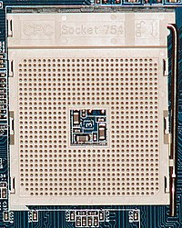
Socket 754
support for a single channel memory controller (64-bits wide) with maximum of 3 DIMMs (no dual channel support)
lower HyperTransport speed (800 MHz Bi-Directional, 16 bit data path, up and downstream)
lower effective data bandwidth (9.6 GB/s)
lower motherboard manufacturing costs
Although AMD has promoted Socket 754 as a budget platform on the desktop and encouraged mid and high end users to use Socket 939 (and recently Socket AM2) instead, Socket 754 remained for some time as AMD's high end solution for mobile applications i.e. no Socket 939 Athlon 64 CPUs have ever been marketed as a mobile processor, aside from at least the HP zv6000 series. Recently however, Socket S1 has been released and is slated to supersede Socket 754 in the mobile market through its support for dual core CPUs and DDR2 RAM.
Socket 939
It was made available in June 2004 and replaced by Socket AM2 in May 2006. AMD has reduced the production of this socket to focus on current and future platforms although demand is still high. When Socket AM2 chips debuted many people were still using 939 PIN sockets with no intention to immediately upgrade, therefore increasing demand for Socket 939 processors. Recently, the Athlon 64 X2 4200+ model (90 nm process, 2x512 KB L2 cache, 89W, E4 and E6 steppings) was the highest speed processor available in the Socket 939 package. [1].
Both single and dual-core processors were manufactured for this socket under the Athlon 64, Athlon 64 FX, Athlon 64 X2, Sempron and Opteron names. The Opteron 185 and Athlon 64 FX-60, both featuring a 2.6 GHz clock speed and 1 MB of Level 2 cache per core, were the fastest processors manufactured for this socket.
====================================================================

Socket 940
The more common use of Socket 940 is in the Server market. Dual Socket 940 boards use the 200-series Opterons. Four(Common) or Eight(Rare) socketed boards use the 800-series Opterons. The Socket 940 platform is designed for raw power and professional accuracy, not bleeding-edge gaming performance.
There is a new 940-pin socket called AM2. Though the current Socket 940 and the AM2 both share the same number of pins, they are not pin-compatible. That is, a Socket 940 processor will not fit in a AM2 socket. The same is true in reverse; a Socket AM2 processor will not fit in Socket 940. The reason for this is because all 64-bit AMD processors, unlike all current Intel processors, include the memory management functionality not as a discrete chip on the motherboard, but rather on the CPU die itself.[2] That means that, if someone wishes to utilize a newer type of memory (e. g. DDR2 vs. DDR), then AMD would need to manufacture an entirely new microprocessor with entirely new memory management electronics built into the chip in order for that newer memory to be usable. This is exactly the situation here; Socket AM2 is designed for DDR2 memory, whereas Socket 940 is designed for DDR (occasionally called "DDR1") memory. This issue highlights one of the disadvantages of including the memory management functions on the CPU die itself. However, performance benchmarks suggest a significant performance increase by doing so, hence AMD's decision to take this design route.
For somewhat related reasons, Socket 939 processors cannot be used in Socket 940 motherboards, even though both Socket 939 and Socket 940 CPUs support the same DDR (aka "DDR1") memory. The distinction here is that Socket 940 requires more expensive registered memory, whereas Socket 939 uses less expensive unbuffered memory. There are also issues of electrical capacitance which lead to four-layer vs. six-layer motherboards (the latter are slightly more expensive to manufacture), which was the reason for the genesis of Socket 939; Socket 940 requires six-layer motherboards. This pin-incompatibility was known to cause some frustration when AMD moved the Athlon 64 FX processor, their premier gaming platform, from a Socket 940 (Opteron 1xx) basis to Socket 939; users who wanted more speed needed to purchase and install an entirely new motherboard. AMD's motivation for Socket 939 was entirely driven by perceived total system cost. However, even after this socket change, the Athlon 64 FX series remained a relatively high cost option, even at times slightly higher than a comparable Socket 940 Opteron.[citation needed] Given the Opteron's excellent performance, it was not unheard of for Socket 940 Opteron 1xx sales to actually cannibalize Athlon 64 FX sales, even at times among the FX's target market, gamers.
Given AMD's recent proliferation of CPU socket platforms, questions about Socket 940's longevity abound on the Internet. Socket 940 was, from the start, primarily geared toward server and higher-end workstation markets, where purchasing decisions are traditionally conservative and customers are known to depreciate (and thus use) their existing gear over at least a five-year cycle. Thus, AMD's plans for Socket 940 stretch out several years into the future, and longevity for this platform is expected to be relatively long. As an example, Socket 5, made famous by the Intel Pentium processor, was in active manufacture, in various backwards-compatible forms including Super Socket 7, for over five years. Socket 370, championed by Intel's Pentium III and Celeron lines, lasted for a similar time frame.[citation needed]
Note that, regardless of the socket form factor, all 64-bit AMD processors will run all of the same software; they are all fully binary-compatible.

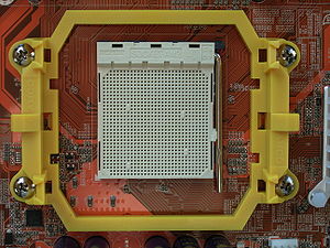
Socket A (also known as Socket 462)
AMD recommends that the mass of a Socket A CPU cooler not exceed 300 grams (10.6 ounces). Heavier coolers may result in damage to the die when the system is not properly handled.
Socket A has been discontinued in favor of Socket 754, Socket 939, and recently Socket AM2, except for its use with Geode NX processors. However, microprocessors and motherboards from many vendors are still available.
====================================================================

The Socket AM2,
AM2 processors are incompatible with 939 motherboards and vice versa, and although it has 940 pins, it is incompatible with Socket 940[1]. DDR2 can transfer more data per clock cycle, but suffers from higher latencies, while drawing less power than DDR memory, which the previous Socket 939 supported. AnandTech reported that Socket AM2 system performance was 0-7% faster than Socket 939 equivalents, with most applications about 2% faster [2][3], despite having over 30% greater memory bandwidth due to DDR2 support.
The first processor cores to support socket AM2 are the single-core Orleans (Athlon 64) and Manila (Sempron), and the dual-core Windsor (Athlon 64 X2 and Athlon 64 FX). Most processors on Socket AM2 include SSE3 instructions and were developed with 90 nanometer technology. Recent models feature 65 nanometer technology (to compete with Intel and their 65nm cpus).
Socket AM2 will support AMD Phenom processors.
Socket AM2 is a part of AMD's next generation of CPU sockets, along with Socket F for servers and Socket S1 for mobile computing.
There are also single-socket Opteron processors available for AM2.[4]
Socket AM3 is a part of AMD's next generation of CPU sockets.
AMD has confirmed that AM3 processors will work in AM2 motherboards; however, AM2 processors will not be compatible with AM3 motherboards. This is because AM2 chips lack the proper memory controller for DDR3 memory (since AMD chips have the memory controller directly on the processor itself, instead of on the Northbridge), and AM3 processors will have a memory controller that supports both DDR2 and DDR3 (though it lacks the capability of running both at the same time). This has the benefit that buyers of current Socket AM2 motherboards will be able to freely upgrade to AM3 processors. They will not enjoy DDR3 memory without a AM3/DDR3 board, but they can take advantage of other features of faster processors, ensuring AM2 boards a longer life than without the compatibility. Revealed from official presentations [1], Socket AM3 will also include DDR2 SDRAM support, and, depending on the adoption rate of DDR3 SDRAM, there is also the possibility to support both SDRAM standards.
Socket AM3 is assumed to be introduced with AMD's next generation processors based on the new microarchitecture.
Socket F is a CPU socket designed by AMD for its Opteron line of CPUs. The socket has 1207 pins, and was released on August 15, 2006[1].
Socket F is primarily for use in AMD's server line, and will be considered to be in the same socket generation as Socket AM2, which will be used for the Athlon 64 and Athlon 64 X2; as well as Socket S1, to be used for Turion 64 and Turion 64 X2 microprocessors. Such socket generations are intended for DDR2 support.
Socket F does not support Fully Buffered DIMM. Processors planned for Socket F will also likely support DDR3 and other technologies, like XDR-DRAM. But when such RAM is used on an FB-DIMM, no motherboard or CPU change is necessary to support the new RAM, as all FB-DIMMs use the same DRAM slots regardless of the RAM employed. This overcomes the old drawback of the Hammer architecture, with its integrated memory controller necessitating the replacement of the (potentially very expensive) CPU to support a new memory type. However, AMD has removed FB-DIMM from its roadmap recently.
[edit] AMD Quad FX platform
Main article: AMD Quad FX platform
Socket F is the base for the AMD Quad FX Platform (referred to as "4x4" or "QuadFather" prior to release), unveiled by AMD on November 30, 2006. This modified version of Socket F, named Socket 1207 FX by AMD, and Socket L1 by NVIDIA, allows for dual-socket, dual-core (four effective cores and eight effective cores in the future) processors in desktop PCs for home enthusiasts.
Socket S1
is the CPU socket type used by AMD for their Turion 64, Athlon 64 Mobile and later Sempron processors, which debuted with the dual core Turion 64 X2 CPUs on May 17, 2006. Socket S1 has 638 pins, and replaces the existing Socket 754 for laptops. It has been expected that desktop motherboards will appear using Socket S1, much as boards using the Pentium M's Socket 479 are on the market.
Socket S1 includes support for dual-channel DDR2 SDRAM, dual-core mobile CPUs, and virtualization technology, to compete with the mobile Intel Core 2 processor series.
Socket S1 is a part of AMD's next generation of CPU sockets, along with Socket F (servers) and Socket AM2 (desktop).

====================================================================
eNd
.JPG)
No comments:
Post a Comment